
Techno-Economic Comparison of 2.5D vs. 3D Packaging: Which to Choose When?
Advanced packaging has become the place where semiconductor scaling is now negotiated, and two of its most important options are 2.5D and 3D packaging. Both are powerful forms of heterogeneous integration, but they solve different problems, carry different risks, and make sense at different points in a product roadmap. The real question is not which one is better in the abstract. It is which one gives the best balance of performance, cost, yield, thermal behavior, and manufacturability for a specific system.
That is why a techno-economic comparison matters. Engineers may be tempted to start with bandwidth or latency, while business teams may start with cost. In reality, both views are incomplete if they are taken alone. A good packaging choice is one where the technical gains justify the economic burden. Sometimes that means the broader, more flexible 2.5D route. Sometimes it means the denser, more aggressive 3D path. Often it means recognizing that the right answer depends on the product’s volume, thermal envelope, schedule, and maturity.
What 2.5D and 3D Really Mean
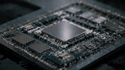
2.5D packaging places multiple dies side by side on an interposer or other high-density routing layer. The interposer acts as a very fine wiring platform, letting logic dies and memory stacks communicate with much higher bandwidth and lower latency than traditional board-level packaging. It is especially well suited to large AI accelerators, high-performance computing devices, and chiplet-based architectures that need strong horizontal connectivity.
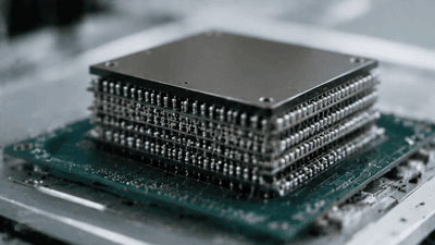
3D packaging goes a step further. Instead of arranging dies horizontally, it stacks them vertically and connects them through TSVs or hybrid bonding. This creates the shortest possible interconnects, which can dramatically reduce distance, power, and latency. In theory, 3D is the more elegant architecture. In practice, it also introduces much harder thermal, mechanical, and manufacturing challenges.
So the basic distinction is simple: 2.5D stretches sideways, 3D builds upward. But the business consequences are not simple at all.
The Technical Appeal of 2.5D
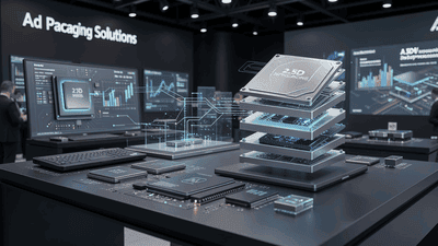
2.5D has become the workhorse of high-end heterogeneous integration because it offers a strong balance of performance and manufacturability. The package can support very high memory bandwidth, especially when large logic dies are paired with multiple HBM stacks on a silicon interposer. The structure is complex, but not so complex that the yield and thermal penalties become unmanageable for many commercial products.
One of 2.5D’s biggest strengths is thermal practicality. Because the dies sit side by side, heat can escape more easily than in a vertically stacked 3D structure. That gives package designers more room to work with cooling solutions and makes system qualification less painful. It also simplifies test access compared with stacked structures, since chiplets can often be validated individually before final assembly.
This makes 2.5D especially attractive when the product needs high performance but also has strict schedule, reliability, or manufacturing constraints. It is a strong option when the design needs heterogeneous integration across multiple process nodes or vendors, but does not need the absolute density of vertical stacking.
The Technical Appeal of 3D
3D packaging is the bolder choice. By stacking dies vertically, it shortens interconnects to the extreme and unlocks the highest density of integration. For some applications, that means lower power, lower latency, and a much smaller footprint. It is especially compelling when the architecture demands the closest possible coupling between dies, such as logic-on-cache, logic-on-memory, or future memory-centric structures.
The promise of 3D is easy to understand: if side-by-side is good, then directly on top should be better. In a lot of ways, that is true. But the technical beauty of 3D hides a brutal reality. Heat removal becomes much more difficult. Die thickness and alignment tolerances get tighter. Stack yield becomes a product of multiple good dies, not just one. And as the stack grows taller, reliability questions multiply.
This makes 3D more attractive when density matters more than almost anything else. It is ideal when footprint is limited, bandwidth and latency are absolutely critical, and the business case can absorb the extra complexity.
The Cost Side of the Equation
If 2.5D and 3D were judged only on technical elegance, 3D might win more often. But technology decisions are rarely made in a vacuum. Cost changes the picture quickly. 2.5D generally requires a silicon interposer or high-density redistribution layer, which adds expense, but the flow is relatively well understood and the yield learning curve is more mature. That makes it easier to scale for certain high-value applications.
3D packaging is usually the more expensive option. It adds extra steps such as TSV formation, fine-pitch alignment, stacking, and in some cases hybrid bonding. Each step introduces cost and risk. If one layer fails, the entire stack can become unusable, which means the effective yield can fall faster than in 2.5D. For low- to mid-volume products, that can be a serious economic obstacle.
The techno-economic question, then, is not whether 3D gives better density. It clearly does. The question is whether that density is worth the extra process complexity and cost. In many products, especially early in a market cycle, the answer is no. The architecture may be technically feasible, but not commercially compelling.
Yield Is the Hidden Multiplier
Yield is where the comparison becomes very real. In 2.5D, the system yield depends on the interposer and the die assembly process, but individual dies can often be known good before final assembly. That helps reduce risk. In 3D, the stack yield becomes multiplicative. Multiple dies, multiple interfaces, and often more constrained test access all combine to make defect management much harder.
This matters because yield has a direct impact on effective cost. A package with a slightly lower manufacturing cost but much poorer yield can end up being more expensive overall. That is one reason 2.5D often looks better in the early phases of technology adoption. It offers a more forgiving path to advanced packaging and heterogeneous integration.
3D can still win, but usually only after process maturity improves, test strategies get better, and volume justifies the investment. In other words, 3D often looks like the future, while 2.5D often looks like the present.
Thermal Trade-Offs
Thermal behavior is one of the clearest dividing lines between 2.5D and 3D. Side-by-side integration in 2.5D gives heat more room to escape, which simplifies cooling. This is one of the reasons 2.5D is so popular in AI and HPC packages, where large dies and HBM stacks generate significant heat but still need manageable thermal paths.
In 3D, heat sources are stacked vertically, which creates hotspots and makes thermal extraction much harder. Even if the electrical path is better, the thermal path is worse. That can force lower clock speeds, more complex cooling solutions, or stricter power limits. In some cases, the thermal penalty outweighs the electrical gain.
This is why 3D is not automatically the “best” option for every high-performance product. If the thermal envelope is tight and the package must run continuously under heavy load, 2.5D may be the safer and cheaper choice. 3D becomes more attractive when the performance density gain is worth the extra thermal engineering effort.
Testing and Qualification
Another big difference is testability. 2.5D is generally easier to test because the dies are assembled in a more accessible layout. Chiplets can often be validated as known-good dies before final integration, and the package can be tested in stages. That reduces risk and shortens the feedback loop.
3D is harder. Once dies are stacked, access becomes more limited. Test strategy must be carefully designed upfront, often with more built-in self-test, more redundancy, and more sophisticated diagnosis. Qualification also becomes more demanding because the package must prove long-term reliability across multiple thermal and mechanical interfaces.
This test complexity has a direct economic impact. Longer test times, more elaborate design-for-test features, and higher scrap risk all raise the true cost of 3D. So even if the bill of materials looks attractive in a narrow sense, the full techno-economic picture may favor 2.5D until the stack technology matures.
When 2.5D Makes More Sense
2.5D is often the better choice when the design needs high bandwidth, moderate integration density, and manageable risk. It is a strong fit for AI accelerators, large GPUs, network switches, and chiplet-based HPC systems where HBM integration is critical and the package can tolerate a broader footprint.
It also makes sense when:
- The product is high value but not so high value that a very expensive 3D stack is justified.
- Thermal management must remain relatively straightforward.
- Different dies from different process nodes need to coexist in one package.
- Time to market matters and process maturity is important.
In these situations, 2.5D often delivers the best total economics. It is advanced enough to unlock heterogeneous integration, but not so extreme that it overwhelms the rest of the design flow.
When 3D Makes More Sense
3D is the right answer when density and interconnect proximity are the main goal and the application can bear the complexity. It becomes more attractive when the package footprint must be minimized, when latency must be pushed down as far as possible, or when stacking creates a clear architectural advantage that 2.5D cannot match.
3D is especially compelling for:
- Very high-density memory-centric architectures.
- Logic-on-cache or logic-on-logic stacks where vertical integration creates real system value.
- Roadmaps that demand future scalability in vertical form factors.
- Products where power efficiency per bit or per operation is the overriding priority.
But even then, the decision has to be grounded in economics. If the stack will only ship in modest volumes, or if the thermal and test penalties are too severe, 3D may still be too costly despite its performance promise.
A Practical Decision Framework
A useful way to choose between 2.5D and 3D is to ask a sequence of questions:
- How much bandwidth and latency improvement does the product really need?
- Is thermal headroom available for vertical stacking?
- Can the business tolerate higher manufacturing complexity and lower initial yield?
- Does the product volume justify a more expensive stack?
- Is the roadmap likely to benefit from a more compact form factor in future generations?
If the answer to most of those questions points toward caution, 2.5D is probably the better economic choice. If the answer points toward extreme density and long-term strategic value, 3D may be worth the risk. This is not a moral decision. It is a portfolio decision.
Technology Maturity and Learning Curve
2.5D has had more time to mature, and that matters. As with most semiconductor technologies, learning curves lower costs over time. Process control improves, materials stabilize, tool availability increases, and design teams get better at making the architecture yield-friendly. That gives 2.5D a real advantage today.
3D is on a steeper learning curve. It promises more, but it still needs better process maturity and broader ecosystem support before it becomes a mainstream economic choice. Over time, that may change. For now, however, 3D is usually reserved for the cases where the value of vertical integration is clear enough to justify the added risk.
Conclusion
The techno-economic comparison between 2.5D and 3D packaging is really a comparison between two different ideas of system building. 2.5D offers a more practical path to heterogeneous integration with strong bandwidth, better thermals, and more manageable cost and yield. 3D offers the most compact, fastest, and most vertically integrated future, but at a much higher level of complexity and risk.
That is why the answer to “which to choose when?” is always contextual. If the product needs a strong balance of performance and manufacturability, 2.5D is often the smarter choice. If the product needs the absolute highest integration density and can justify the cost, 3D becomes the better fit. In advanced packaging, the right answer is the one that aligns architecture, thermal design, yield strategy, and business reality. The art is knowing where that line is.





